- 您现在的位置:买卖IC网 > Sheet目录335 > ISO1I811T (Infineon Technologies)ISOLAT DGTL 500VAC 8CH 48TSSOP
ISO1I811T
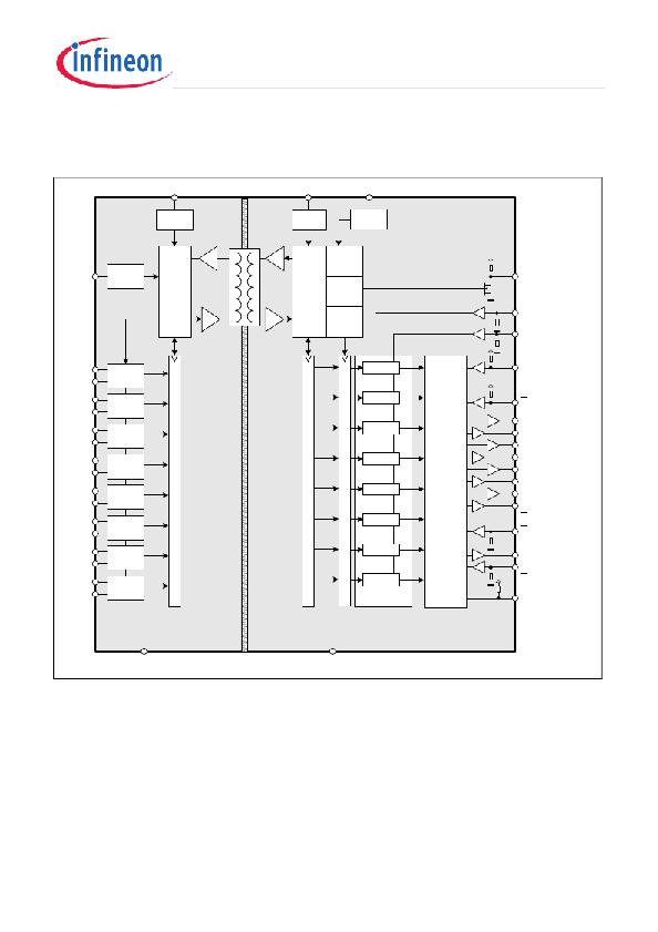
Pin Configuration and Functionality
1.2.2
Pins of Serial and Parallel logic Interface
Some pins are common for both interface types, some others are specific for the parallel or serial access.
VCC (Positive 3.3 / 5V logic supply)
VCC supplies the output interface that is electrically isolated from the sensor input stage. The interface can be
supplied with 3.3 / 5V.
GND (Ground for VCC domain)
This pin is the ground reference for the uC-interface that is supplied by VCC.
ROSC (Clock Adjustment)
A high precision resistor has to be connected between ROSC and GND to guarantee the frequency accuracy of
the sampling clock. For details see Chapter 3.3 .
ERR (Error Output)
The low active ERR signal contains the OR-wired information of the sensor input missing voltage (MV) detection
and the internal data transmission failure detection unit. The output pin ERR provides an open drain functionality.
A current source is also connected to the pin ERR. In normal operation the signal ERR is high. See Chapter 3.5
for more details.
DS0, DS1 (Filter Select)
The internal filter delay can be selected by pulling those pins to VCC or to GND (see Table 10 ). These pins are
for static configuration (pin-strapping).
CS (Chip Select)
When this pin is in a logic Low state, the IC interface is enabled and data can be transferred.
SEL (Serial or Parallel Mode Select)
When this pin is in a logic High state, the IC operates in Serial Mode. For Parallel Mode operation the pin has to
be pulled into logic Low state. This pin has an internal Pull-UP resistor.
The following pins are provided by the parallel interface
D7:D0 (Data output bit7 ... bit0)
Th e pins D0 .. D7 are the outputs for data read.
RD (Read Select )
By pulling this pin down, a read transaction is initiated on the data bus and the data becomes valid.
The following pins are provided by the serial interface
SCLK (Serial interface shift clock)
Output data is updated with the falling edge of this input clock signal.
SDI (Serial interface input data)
SDI is put into a FIFO dedicated to the sensor data bits (no internal registers Write operation supported, only daisy
chain). Input data is sampled with the rising edge of SCLK.
SDO (Serial interface data)
SDO provides the sensor data bits.
Data Sheet
9
Revision 2.0, 2012-06-14
发布紧急采购,3分钟左右您将得到回复。
相关PDF资料
ISO7221AQDRQ1
IC DGTL ISOLATOR 1MBPS DL 8SOIC
ISOBAR4 ULTRA
SURGE SUPPRSSR 4OUT 6'CORD W/LED
ISOBAR6 ULTRA
SURGE SUPPRSSR 6OUT 6'CORD W/LED
ISOBAR6DBS
SURGE SUPP DSS 6OUT 6'CORD W/LED
ISOBAR6ULTRAHG
SURGE SUPP 6OUT 15'CORD HOSP GRD
ISOBAR6
SURGE SUPPRSSR 6OUT 6'CORD
ISOBAR8 ULTRA
SURGE SUPPR 8OUT 12'CORD W/LED
ISOBLOK2-0
SURGE SUPP ISOBAR 2 OUT/DIRECT
相关代理商/技术参数
ISO1I811TXUMA1
制造商:Infineon Technologies AG 功能描述:ISOFACE - Tape and Reel 制造商:Infineon Technologies AG 功能描述:IC DGTL ISO 8CH PAR SER 48TSSOP
ISO1I811TXUMA1/SAMPLE
制造商:Infineon Technologies AG 功能描述:ISOFACE - Tape and Reel
ISO1I813T
功能描述:ISOLATOR DGTL 500VAC 8CH 48TSSOP RoHS:是 类别:隔离器 >> 数字隔离器 系列:ISOFACE™ 标准包装:66 系列:iCoupler® 输入 - 1 侧/2 侧:2/2 通道数:4 电源电压:3.3V,5V 电压 - 隔离:2500Vrms 数据速率:25Mbps 传输延迟:60ns 输出类型:逻辑 封装/外壳:20-SSOP(0.209",5.30mm 宽) 供应商设备封装:20-SSOP 包装:管件 工作温度:-40°C ~ 105°C
ISO1I813TXUMA1
制造商:Infineon Technologies AG 功能描述:Isolated 8 Channel Digital Input 48-Pin TSSOP 制造商:Infineon Technologies AG 功能描述:ISOFACE - Tape and Reel 制造商:Infineon Technologies AG 功能描述:ISOLATOR DGTL 500VAC 8CH 48TSSOP
ISO2
制造商:未知厂家 制造商全称:未知厂家 功能描述:ASIC
ISO212
制造商:BB 制造商全称:BB 功能描述:Low Cost, Two-Port Isolated, 1500Vrms ISOLATION AMPLIFIER
ISO212JP
制造商: 功能描述: 制造商:undefined 功能描述:
ISO212JP-15
制造商:BB 制造商全称:BB 功能描述:Low Cost, Two-Port Isolated, 1500Vrms ISOLATION AMPLIFIER
